Search results for keyword: wafers
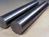
Expansion alloy (GB/T14985-1994)
Expansion alloy (GB/T14985-1994)
Expansion alloy is an important metal material widely used in our daily life. It is a material composed of metal base and special alloy elements, which has the effect of thermal expansion. Generally speaking, expansion alloy is a kind of alloy with good thermal ex......

 1055
1055  Samantha
lithography
Laser Engraving
Laser engraving is one of the most frequently used and versatile techniques for producing accurately created etched effects in metal, glass, and non-metallic materials. Laser engraving is an impact-less, non-contact process, which leads to excellent precision and quality when engr......
Common Defects of Nitriding (Soft Nitriding)
Leakage of N2 in NF3 Etching
As the need for complex semiconductor wafers and advanced packaging technologies continues to grow, so does the need for sophisticated high-throughput chemical etching processes. Nitrogen trifluoride (NF3) is a key etchant used in the semiconductor industry, as it is ......
Desiliconization agent
Etching of Silicon wafers
Silicon wafers are a crucial component of the semiconductor industry. They are typically formed from pure silicon material, which is sliced into thin circular disks. Each one of these disks, which are typically a few millimeters thick, comprise of a series of integrated ......
physical vapor deposition
Physical Vapor Deposition
Physical vapor deposition (PVD) is a technique that is used to coat surfaces with thin layers of metal, polymer, or ceramic particles. The Vacuum Coating Technology (VCT) Group defines PVD as “a process where the material is evaporated in a vacuum and is then transferre......
Japanese metal silicon
Japan Metal Silicones
Japan metal silicones are an advanced type of silicone technology used for various applications in metal fabrication, engineering and industrial processes. Largely since the 1990s, Japanese companies have been leading the charge in the development and application of metal s......
niobium aluminum
Molybdenum-Rhenium-Aluminum Alloys
Molybdenum-Rhenium-Aluminum (MRA) alloys are a type of alloy with a combination of copper and aluminum that provides superior strength and corrosion-resistance. MRA alloys are used in a variety of industries for their superior properties such as high strength, re......
gallium arsenide
Gallium arsenide (GaAs) is a compound of the elements gallium and arsenic. It is an important semiconductor material used in most high-speed and high-frequency electronic devices. GaAs was discovered in 1915 by German chemist Alfred Stock and is the most commonly used compound semiconductor of the ......
Semiconductor Wafer Grinding
,不写中文
Semiconductor wafer grinding is a key process in the production of semiconductor devices. The aim of this grinding process is to produce semiconductor wafers with a very close-to-ideal surface profile. This is achieved by using abrasive materials such as diamond or silicon carbide and gr......
semiconductor heterojunction
Heterojunction Semiconductor Introduction
The semiconductor heterojunction refers to a junction between two different semiconductor materials. It is a common technique used to construct a semiconductor device for various applications. This can be achieved by either depositing a thin layer of one ......

Popular Entries
- Spanish heat-resistant steel steel grade
- Faults caused by incorrect mixing ratio of gasoline and engine oil
- How lifts work
- overseas trade
- London Exchange Alternative Investment Market
- Zibo Fushan Mining Co., Ltd.
- Brinell/Rockwell hardness conversion table
- Zhangjiagang Rural Commercial Bank
- ГOCT 5949-1975 Specifications for corrosion-resistant, heat-resistant and heat-strength steel bars and cold-worked products
- thermodynamics thermodynamics
- re-election workshop design
- employee satisfaction
- Density of diamond
- Rationalized Global Planning Model
- digital wallet
Recent Updates
- continuous casting
- ГOCT 5949-1975 Specifications for corrosion-resistant, heat-resistant and heat-strength steel bars and cold-worked products
- overseas trade
- shipping
- Korea Xinsheng Shipping Co., Ltd. Shanghai Office
- Hamilton's Protectionist Trade Doctrine
- Rationalized Global Planning Model
- Heckscher-Ohlin model
- black market price
- buy each other
- principle of reciprocal treatment
- The unit that accepts entrusted customs declaration
- reciprocal tariff
- sliding tariff
- digital wallet
- horizontal trade
Trending Keywords


Copyright © 2016 - 2024 by metal-knowledge.com. All rights reserved