,关于硅外延片
Silicon wafer epitaxy is an advanced technique used to produce semiconductor or solid-state devices and is capable of producing high-quality devices. The process is used to create monocrystalline silicon structure by depositing layer upon layer of silicon onto a substrate. Impressively, this process can be used to create devices orders of magnitude more complex than what can be achieved with any other method.
In order to explain how the process works, we need to explore the structure of crystalline silicon. Crystalline silicon has a diamond cubic crystal structure. The atoms in the silicon lattice are arranged such that each atom is covalently bonded to four neighboring atoms, forming a structural unit called a unit cell. Each unit cell is composed of eight atoms and has a cubic shape.
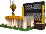
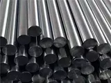
The epitaxy process begins with a single-crystal substrate. This can be made from natural or synthetic single crystalline silicon. The substrate is then cut or ground into circular or rectangular shapes and the surfaces of the substrate is then etched or polished to form a smooth, flat layer. A polymeric sticky material, such as photoresist, may be applied to the substrate to hold the layers of silicon during deposition.
The next step is to deposit the layers of silicon onto the substrate. This involves depositing silicon of a specific thickness only onto a particular region of the substrate. The deposition is accomplished via chemical vapor deposition (CVD), which is a process where the substrate is exposed to certain gases in a reaction chamber. The gases breakdown and deposit their silicon molecules onto the substrate’s surface.
The CVD process ensures that the deposited silicon layers have the same atomic structure, crystal orientation and spacing as the starting substrate. This is known as epitaxial growth, and it is the process that allows for the creation of extremely fine, highly efficient structures such as transistors and diodes.
The deposition process is repeated several times and is also often accompanied by various techniques such as oxidation, diffusion, and dopants. Oxidation is used to introduce oxygen atoms into the deposited layers, which can dramatically alter the electrical performance of these devices. Diffusion is used to introduce other materials into the deposited layers which are designed to influence the movement of electrons. Finally, dopants are introduced to further induce or control the flow of electrons in the structure.
The processing parameters are very precisely controlled throughout the entire process, ensuring that the layers deposited during epitaxy contain no defects or impurities. This is essential as these defects can drastically decrease the quality of the device produced. Once the desired layers are deposited, the substrate is then cut into the desired shape, often using a laser.
Silicon wafer epitaxy is a complex and interesting process capable of producing some of the most advanced semiconductor devices available today. The layers deposited using this process contain no defects and are incredibly thin and efficient, resulting in significantly improved device performance. In addition, the process permits devices more complex than any other method and allows for extremely fine structures. This makes silicon wafer epitaxy an invaluable tool in the production of today’s semiconductor devices.