Introduction
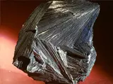
A semiconductor crystal slice, also known as a semiconductor wafer, is a thin slice or plate of semiconducting material typically used in the fabrication of integrated circuits and other microelectronic devices. The slice is cut from a semiconductor substrate such as silicon. These slices are thicker than a typical aluminum foil with a thickness of 200-300 μm and can be as thin as 10 μm. They are also known as wafers of a given diameter. The slices are used to create the most advanced microelectronic components, including transistors, diodes, and logic circuits which are used in computers and other digital electronics.
Advantages
Semiconductor crystals slices have many advantages that make them the materials of choice for designing new microelectronic components. First, they are highly conductive and can be used to create very small and highly efficient devices. Second, because of their thinness and uniformity, they can be used to create devices with very precise tolerances and can enable the device to perform with very low distortion. Finally, they are compatible with both high and low frequency electronic circuitry, which helps designers to reduce the size and power requirements of their chips.
Common Types
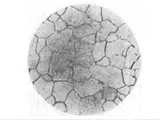
There are three common types of semiconductor crystal slices: monocrystalline silicon, polycrystalline silicon, and amorphous silicon. Monocrystalline silicon slices are composed of a single crystal of silicon atoms arranged in an orderly, three-dimensional lattice. This type of slice is the most commonly used in integrated circuits because it offers superior thermal and electrical performance. Polycrystalline silicon slices are made of randomly arranged crystalline silicon and are typically less expensive than monocrystalline slices. They are used in applications such as photocells and LEDs. Amorphous silicon slices are made of atoms arranged randomly and are used for photovoltaic (solar cell) applications.
Fabrication Process
The fabrication of a semiconductor crystal slice begins with the creation of a “template” for the slice. This template is made by etching a pattern into a substrate such as silicon or gallium arsenide. After the pattern has been created, the substrate is heated until it melts. The molten substrate is then cooled and removed from the template, leaving behind a thin slice of the material. The sliced material is then polished to create a smooth, uniform surface before being tested for electrical properties.
Conclusion
Semiconductor crystal slices are an essential component in the fabrication of microelectronic components. They are highly conductive, uniform, and compatible with high and low frequency circuitry. They are also more cost-effective than other types of materials used in the fabrication of integrated circuits. The fabrication process involves the creation of a template and the molten substrate is cooled and removed from the template, leaving behind a thin slice of material. The sliced material is then polished and tested for electrical properties before being ready for use.